
Bread80 · @bread80
203 followers · 1031 posts · Server mstdn.social
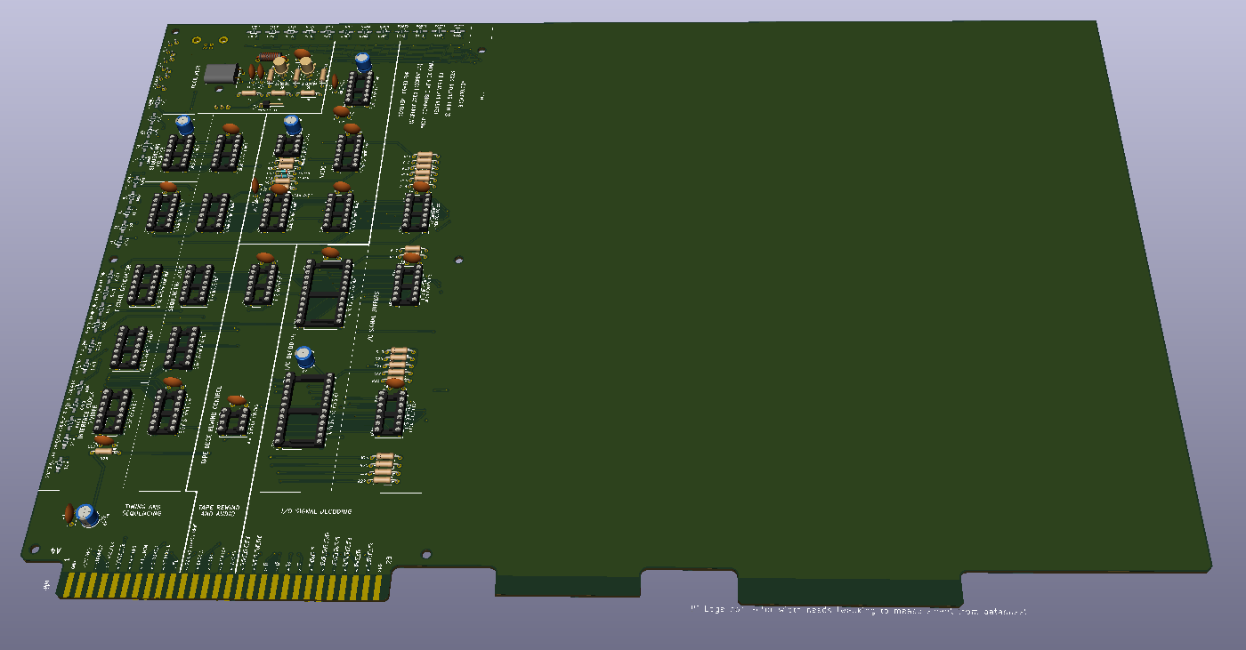
That’s the surface mount soldering finished on the #d2200 memory card. When I say finished, I’ve verified that every LEDs are the same way around. I’ve not checked they’re the correct way around. I think I’ll do some testing before moving onto the through holes. #datapoint #TTLComputer
#ttlcomputer #datapoint #d2200
Bread80 · @bread80
199 followers · 950 posts · Server mstdn.social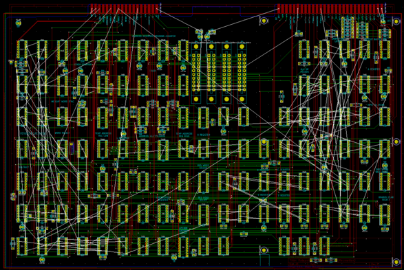
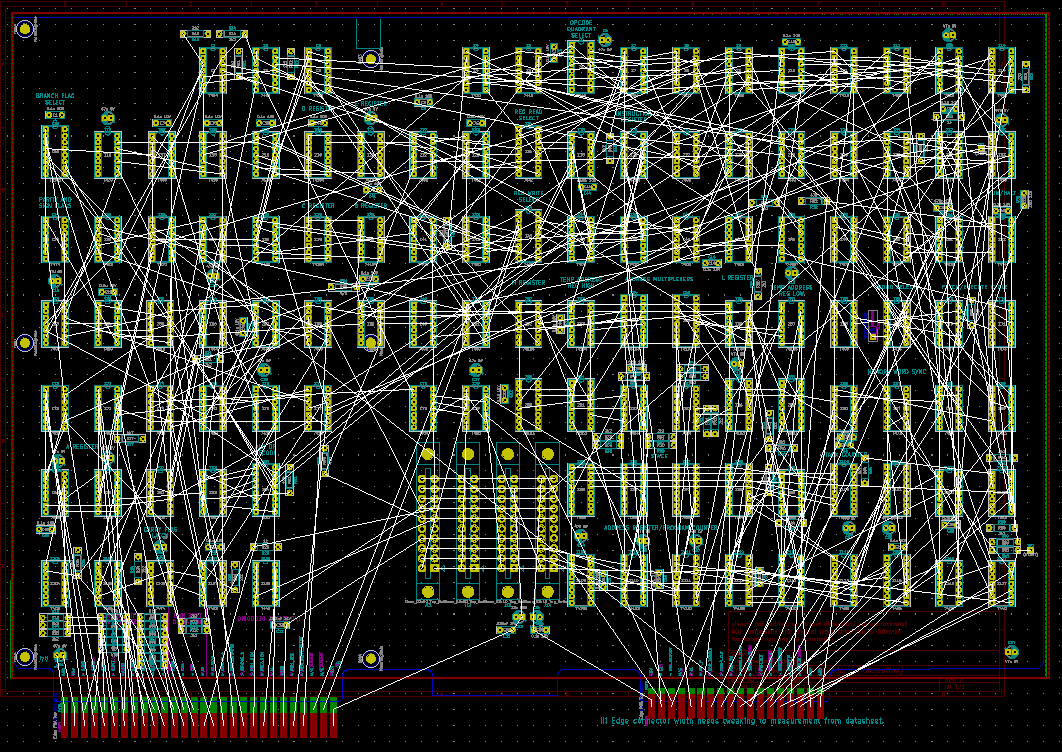
And the current routing status. Nine pages of schematics done. Three left to go.
#ttlprocessor #datapoint2200 #datapoint #d2200
Bread80 · @bread80
195 followers · 924 posts · Server mstdn.social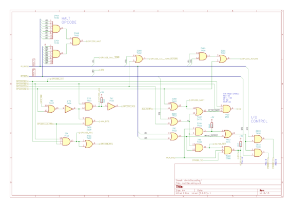
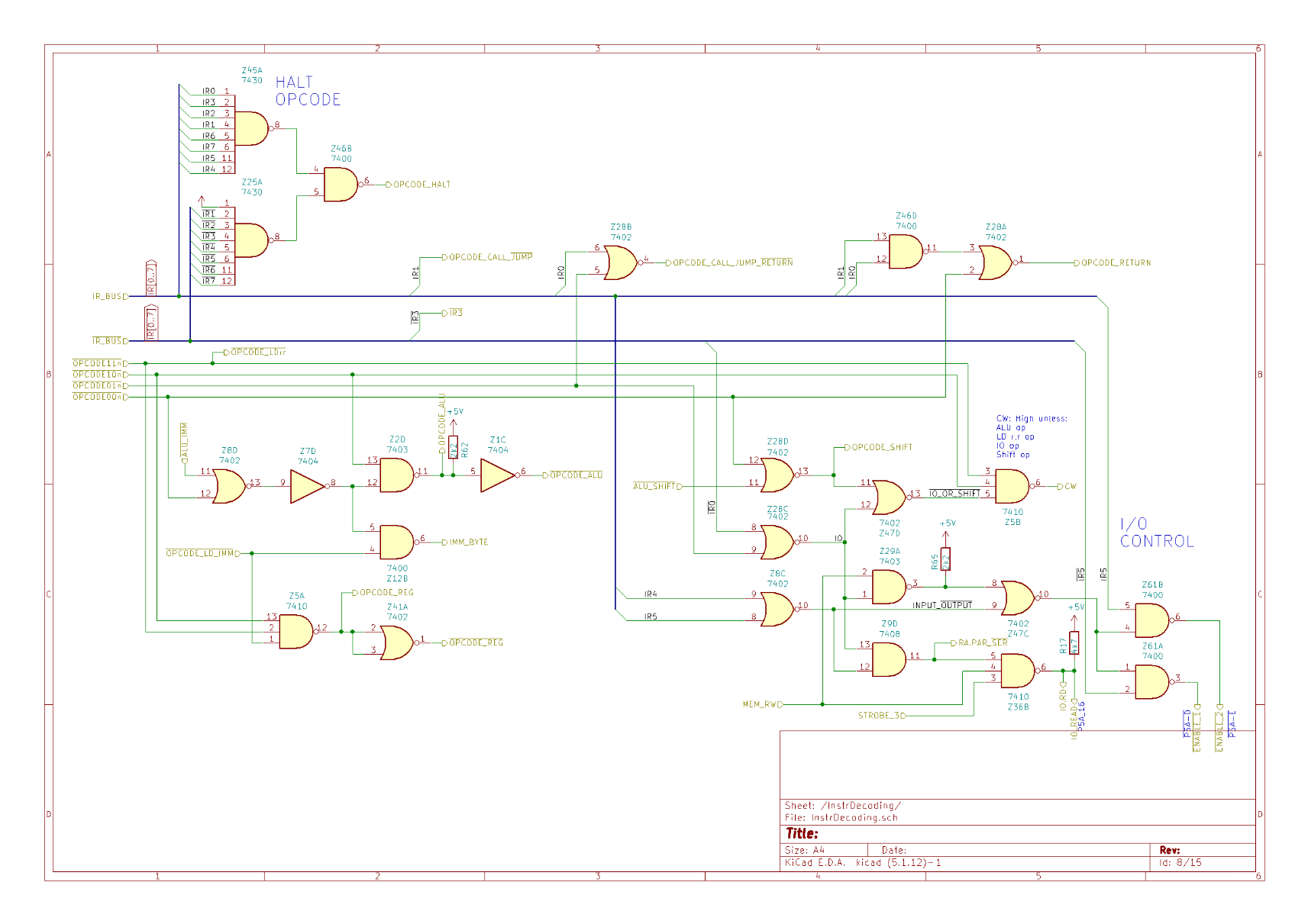
I think that's enough routing for one day. This is the second page of instruction decoding. Here we have:
* HALT opcodes - there's three of them, &00, &01, &ff. I don't know why they felt the need for three. Those octal NANDs are one gate per chip which. But &ff would, otherwise, decode to LD (HL),(HL). Z80 peoples will be proud of that.
* Some branching stuff.
* Some general stuff.
* Shift and I/O stuff.
(I know those comments aren't helpful. I'm tired).
Bread80 · @bread80
195 followers · 924 posts · Server mstdn.socialIf you'd like to compare the Datapoint and Z80 instruction sets I have an article which does exactly that:
https://bread80.com/2022/07/09/comparing-datapoint-2200-8008-8080-and-z80-instruction-sets/
Bread80 · @bread80
195 followers · 924 posts · Server mstdn.social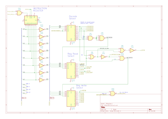
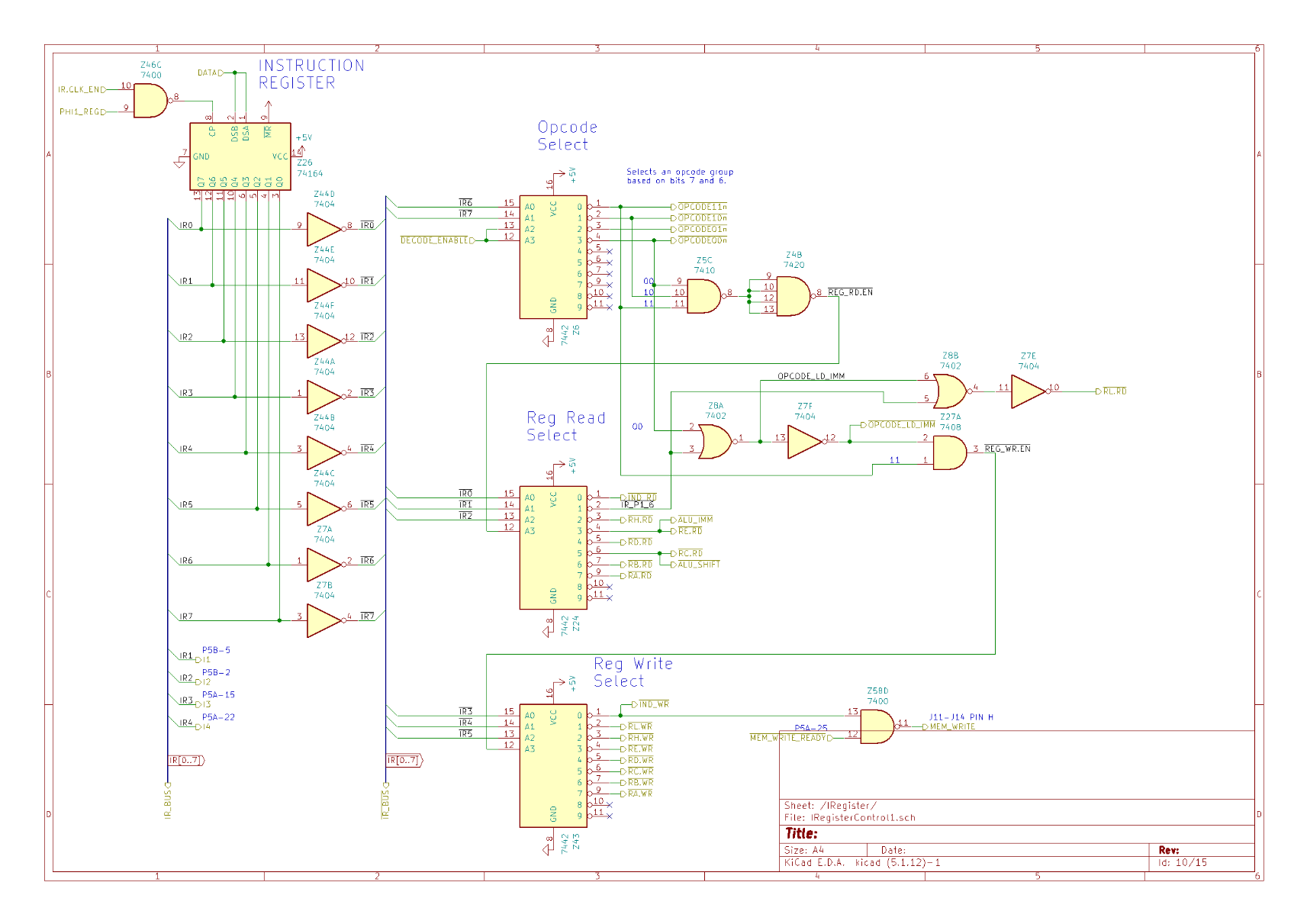
If my ordering for this seems a little random it's because I'm following Kicads page numbering of the schematics. But I'm skipping forward to the instruction register because it produces a tonne of control signals which trace across the board.
Instructions are grouped by bits 7 and 6 of the bytecode. Depending on the opcode bits 4,3,2 and 2,1,0 encode the destination and source registers respectively.
Bread80 · @bread80
195 followers · 924 posts · Server mstdn.social
BTW if you look at the bits of the opcode which are encoding the flags and compare then to the equivalent Z80 opcodes you'll notice they're identical. There are, of course, a lot of similarities between the 2200 and it's great grandchild.
Bread80 · @bread80
195 followers · 924 posts · Server mstdn.social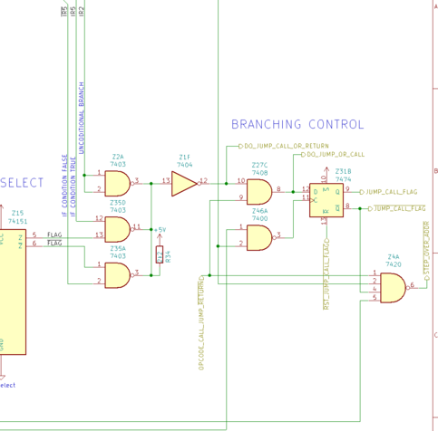
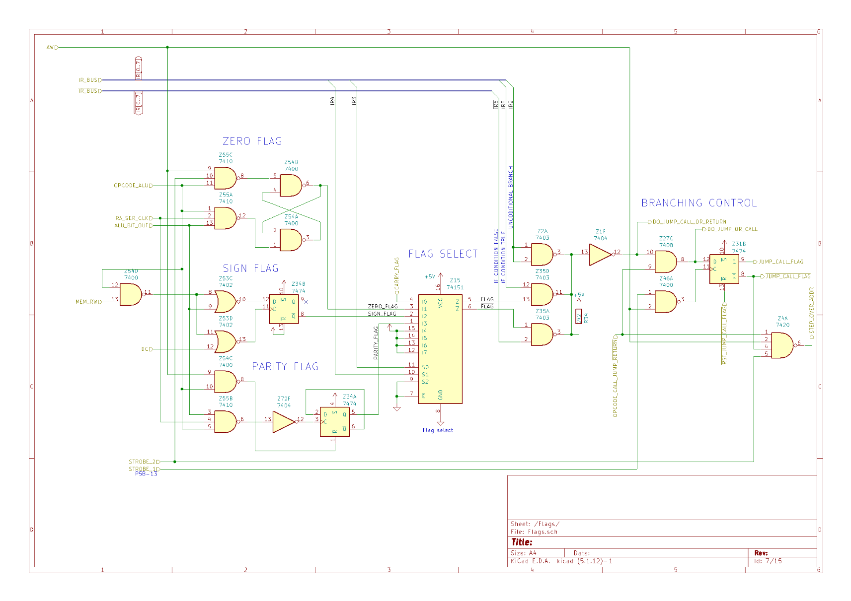
It's worth noting that this circuit functions for every opcode in the instruction register even if it's not a branch instruction.
It's only at the next stage that the processor examines whether the opcode is a jump, call or return and sends signals elsewhere to load an immediate address, push the program counter on the stack or pop a return address off the stack.
#ttlprocessor #datapoint2200 #datapoint #d2200
Bread80 · @bread80
195 followers · 924 posts · Server mstdn.social
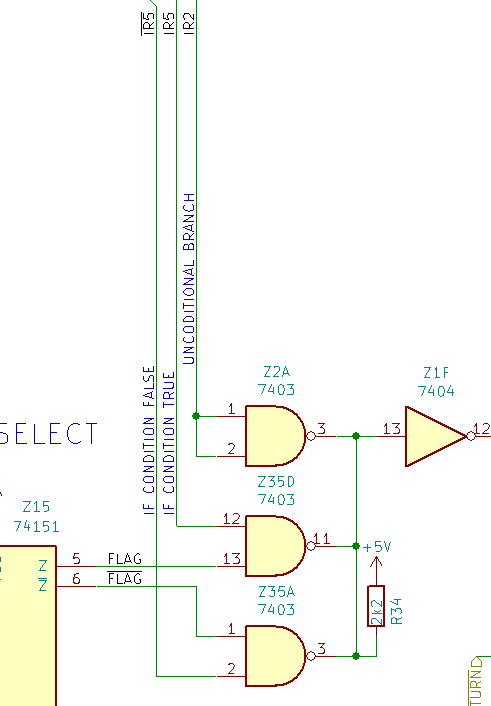
This part of the circuit uses OC gates to select whether a branch needs to be taken. Z35A and Z35D will output zero if the flag matches the if true/if false specified by IR5. In IR2 is high we have an unconditional branch and, in that case, Z2A always drives the signal low.
Examine the circuit and you'll notice it's actually functioning as an OR gate (but with inverted logic). Using a single resistor helps reduce the chip count.
Bread80 · @bread80
195 followers · 917 posts · Server mstdn.social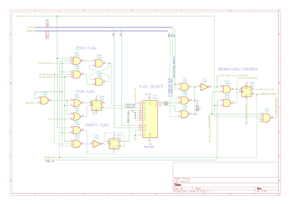
Flags and branch control. This is a nice, easy to understand circuit. It starts with computing the zero, sign and parity flags. Since we have a 1-bit ALU the sign and parity flags are re-evaluated for each bit. Sign flag is just bit 7 of the result. Carry flag circuit is on another page.
IRn are raw bits of the opcode from the instruction register. A multiplexer IC uses IR3 and 4 select a flag to test. IR5 selects for condition true or condition false.
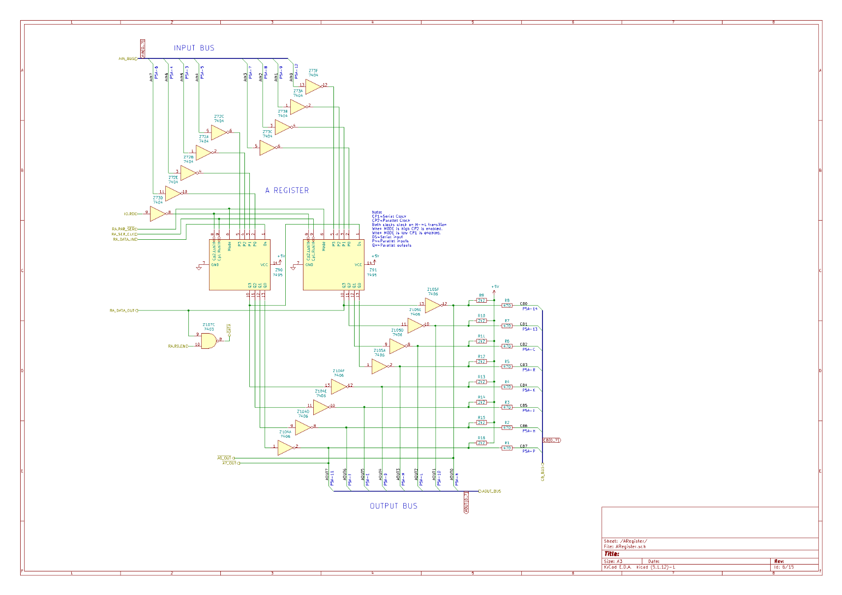
Bread80 · @bread80
195 followers · 917 posts · Server mstdn.social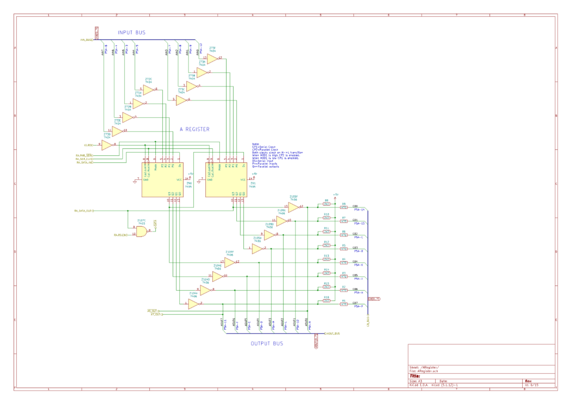
Onto the A register. This uses a pair of 7495 4-bit parallel in, parallel out, shift registers. The top of the schematic is the input bus, the bottom is the two(!) output busses.
While the processor is 1-bit serial it can communicate with other devices over these parallel busses. I'm not sure why there are two output busses though.
On the PCB you're looking at the six chips on the right for the register and input and output buffers/inverters.
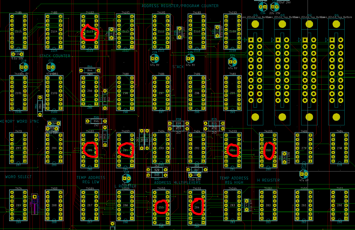
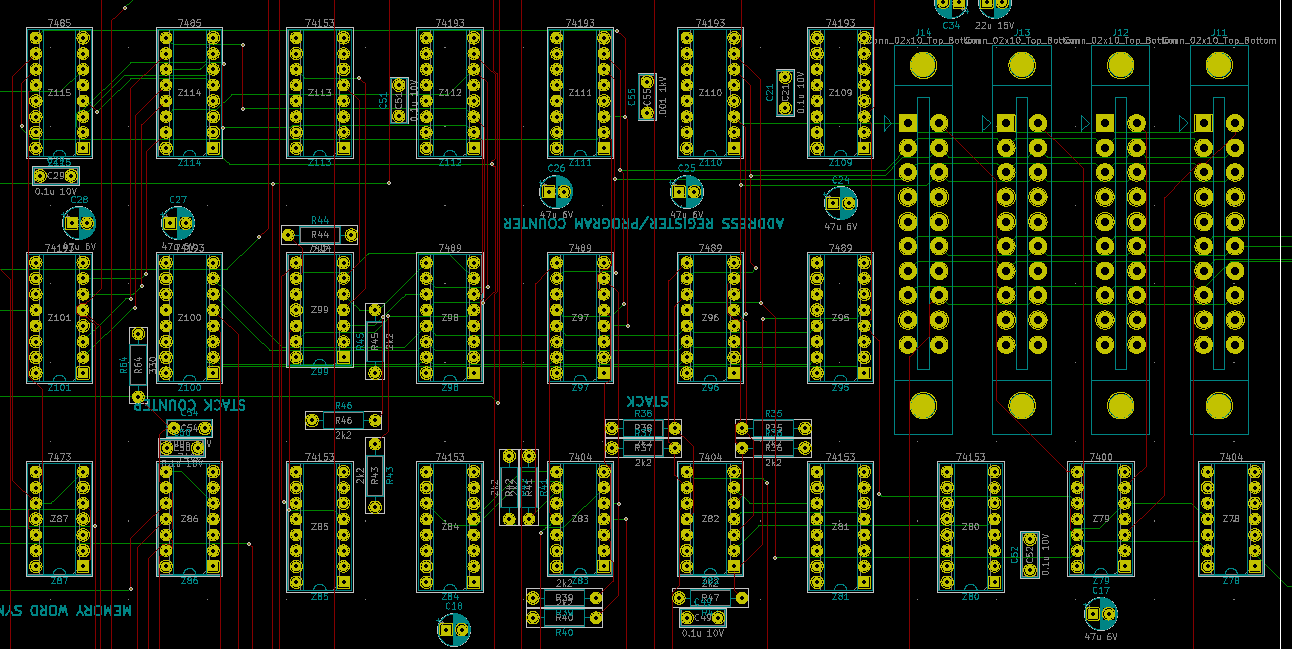
Bread80 · @bread80
195 followers · 917 posts · Server mstdn.social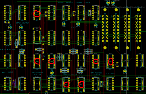
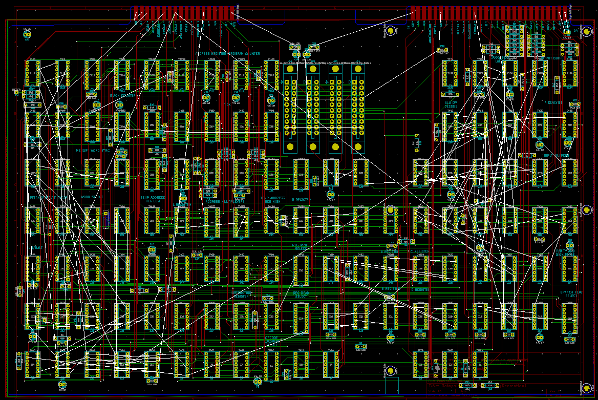
And the mostly routed address related sections of the board. I've marked the 7 multiplexer ICs with red and sorted the silkscreen labels for the other chips.
There's an enjoyable symmetry to those multiplexers - if you ignore Z113.
Routing for now is a case of getting everything connected. I'll tidy later. And I'm leaving space down the middle of ICs to route power and ground. I've never tried this before. I'm hoping it'll be easier than trying to squeeze them in later.
Bread80 · @bread80
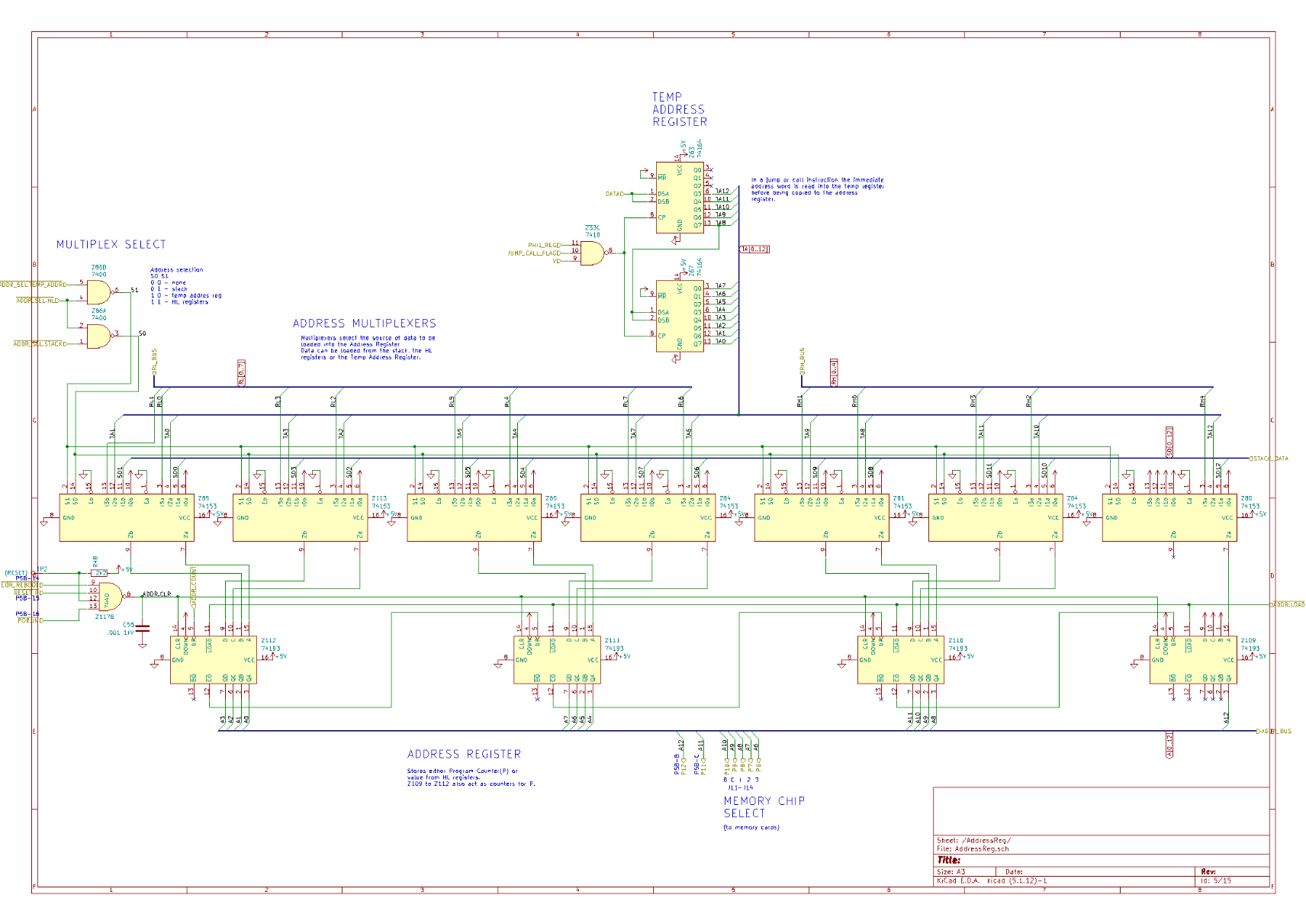
195 followers · 917 posts · Server mstdn.social
And the address multiplexers. Data can be loaded into the address registers from 3 sources: the stack, the H and L registers or the temp address register. The multiplexers select the source.
The Temp Address Register is used when reading a call or jump inline address. These are the only instructions which take an immediate address. All other memory references have to go via the H and L registers.
#ttlprocessor #datapoint2200 #datapoint #d2200
Bread80 · @bread80
195 followers · 917 posts · Server mstdn.social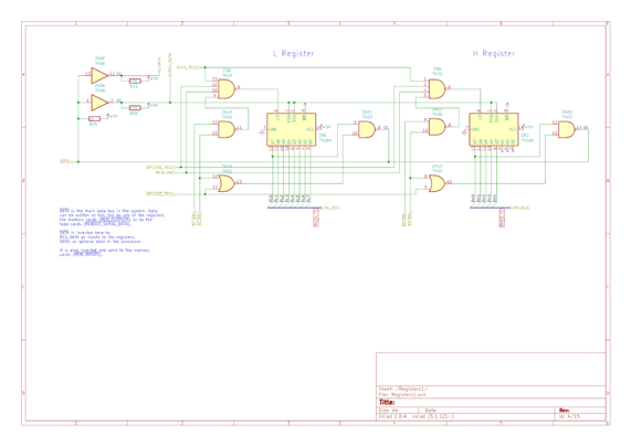
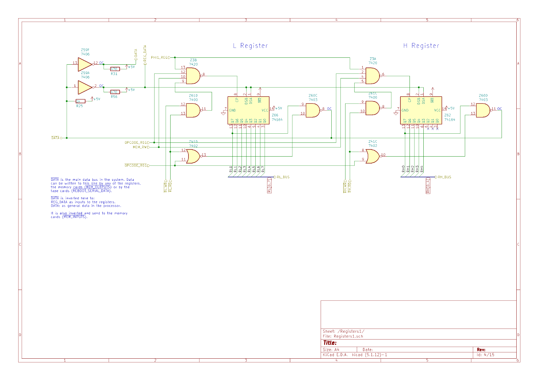
Next up, H and L registers. Probably the simplest schematic of the lot.
These shift registers output to the /DATA bus via an open collector NAND gate. The /DATA line takes output from all the registers, the memory cards, and the tape board - which reads a file on reboot.
Inverters (top left) output to
1) the REG_DATA line which is used as input by the B,C,D,E,H,L registers,
2) the DATA line which is input to everywhere else (IR, ALU, temp addr reg)
Bread80 · @bread80
195 followers · 917 posts · Server mstdn.social
Another page of schematics done - the stack. An A4 page with few external connections and quite quick to route. :phew:
Z95 to 99 are the stack, Z100 the stack up/down counter. Z109 to Z112 are the address register/counters. Z101, 114 and 115 clock the memory until they match the address on A0 to A6. A7 to A10 are sent to the memory cards (top-right) for decoding on the board. Z79 decodes A11 and A12 to select a memory card.
Bread80 · @bread80
195 followers · 917 posts · Server mstdn.socialYou'll notice I've rotated the board 180 degrees in the editor.
Routing it this way is helping me to see where functionality lives. Given the natural viewing angle will be from the front (memory cards at the rear) rotating it now saves me having to relearn the map later.
It is, however, a total mind freak to now see everything upside down.
Another benefit to this: the first page of the schematic is the control stuff. So most of the long, winding, traces should now be done.
Bread80 · @bread80
195 followers · 917 posts · Server mstdn.social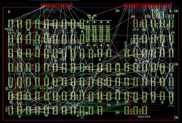
I'm finding the best way to route this is by working through the schematics. The other way, starting with Z1 was challenging due to the length of the traces and the number of destinations.
Doing it this way I can quickly see from the schematic if there's just one or two other pins to visit. That probably sounds long winded but it works form my brain.
Bread80 · @bread80
193 followers · 895 posts · Server mstdn.social
Bread80 · @bread80
193 followers · 894 posts · Server mstdn.social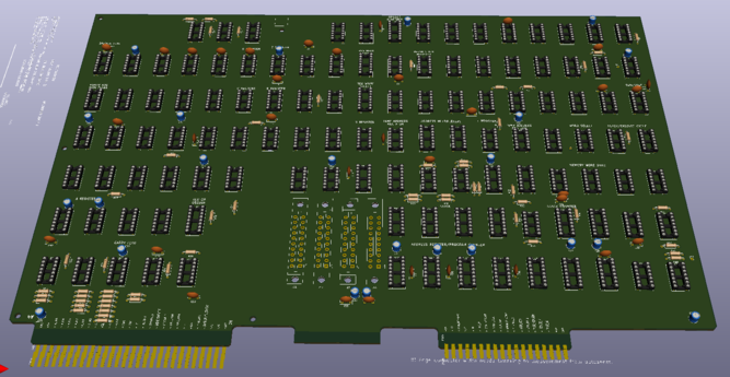
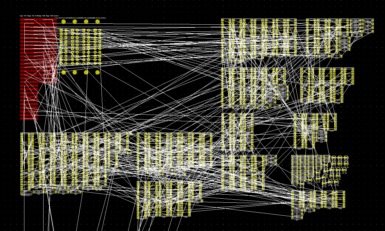
All components placed - to match the positions on the original board. Still some fettling to do on the edge connectors.
I'm now finally realising how ridiculously large this board is. In a way which, for unknown reasons, I'd been completely oblivious to previously.
#ttlprocessor #datapoint2200 #datapoint #d2200
Bread80 · @bread80
193 followers · 894 posts · Server mstdn.social
Footprints imported to the PCB designer. Not actually as scary as I was expecting. Let the fun begin...
Bread80 · @bread80
193 followers · 888 posts · Server mstdn.social
I've copied the Decoder PCB to get the edges of the Processor PCB. I'm using a print out of the decoder PCB and the long edge dimension of the decoder board to work out the scale of the print out.
I can then measure and scale up from the print out.
I'll keep the old decoder components and silk screen for the moment to reuse dimensions and design standards.
#ttlprocessor #datapoint2200 #datapoint #d2200