
mohansus · @mohansus
204 followers · 154 posts · Server newsie.socialIs India booming at 76? GDP’s failure to recover fully indicates otherwise
Is India booming at 76? GDP’s failure to recover fully indicates otherwise
Worth a read for the many "insights" into why #india's #gdp #growth "masks" many "failures" in #structural and #datapoint #terms.
For instance, in absolute terms, the #indianeconomy has grown by 10.1% between 2019-'20 and 2022-'23, which averages an #economicgrowth of around 3-3.5% in "real" numbers.
#india #gdp #growth #structural #datapoint #terms #indianeconomy #economicgrowth

Bread80 · @bread80
203 followers · 1031 posts · Server mstdn.social
That’s the surface mount soldering finished on the #d2200 memory card. When I say finished, I’ve verified that every LEDs are the same way around. I’ve not checked they’re the correct way around. I think I’ll do some testing before moving onto the through holes. #datapoint #TTLComputer
#ttlcomputer #datapoint #d2200
Bread80 · @bread80
199 followers · 950 posts · Server mstdn.social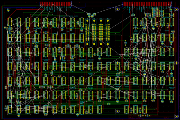
And the current routing status. Nine pages of schematics done. Three left to go.
#ttlprocessor #datapoint2200 #datapoint #d2200
Bread80 · @bread80
195 followers · 924 posts · Server mstdn.social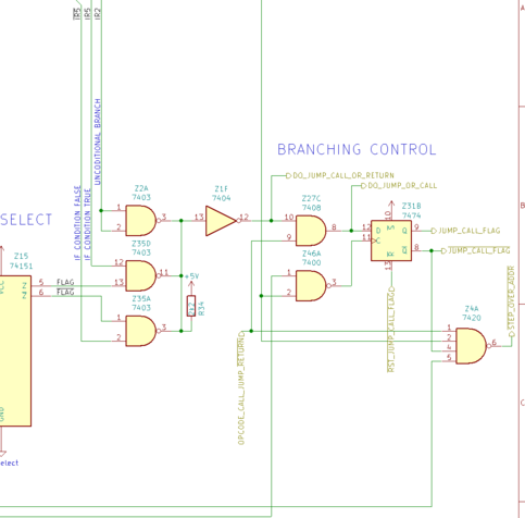
It's worth noting that this circuit functions for every opcode in the instruction register even if it's not a branch instruction.
It's only at the next stage that the processor examines whether the opcode is a jump, call or return and sends signals elsewhere to load an immediate address, push the program counter on the stack or pop a return address off the stack.
#ttlprocessor #datapoint2200 #datapoint #d2200
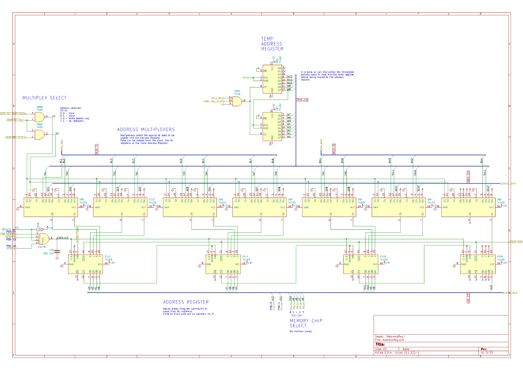
Bread80 · @bread80
195 followers · 917 posts · Server mstdn.social
And the address multiplexers. Data can be loaded into the address registers from 3 sources: the stack, the H and L registers or the temp address register. The multiplexers select the source.
The Temp Address Register is used when reading a call or jump inline address. These are the only instructions which take an immediate address. All other memory references have to go via the H and L registers.
#ttlprocessor #datapoint2200 #datapoint #d2200
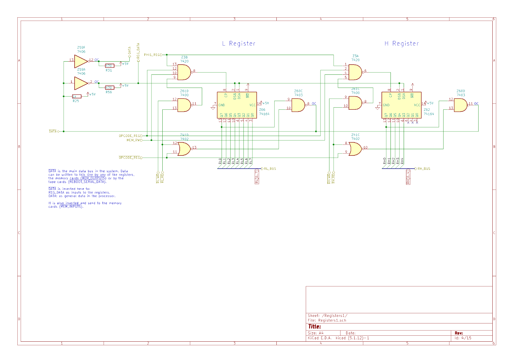
Bread80 · @bread80
195 followers · 917 posts · Server mstdn.social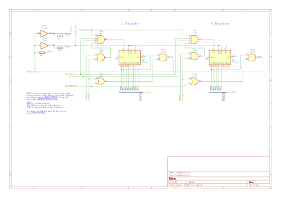
Next up, H and L registers. Probably the simplest schematic of the lot.
These shift registers output to the /DATA bus via an open collector NAND gate. The /DATA line takes output from all the registers, the memory cards, and the tape board - which reads a file on reboot.
Inverters (top left) output to
1) the REG_DATA line which is used as input by the B,C,D,E,H,L registers,
2) the DATA line which is input to everywhere else (IR, ALU, temp addr reg)
Bread80 · @bread80
193 followers · 894 posts · Server mstdn.social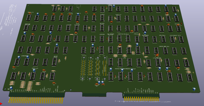
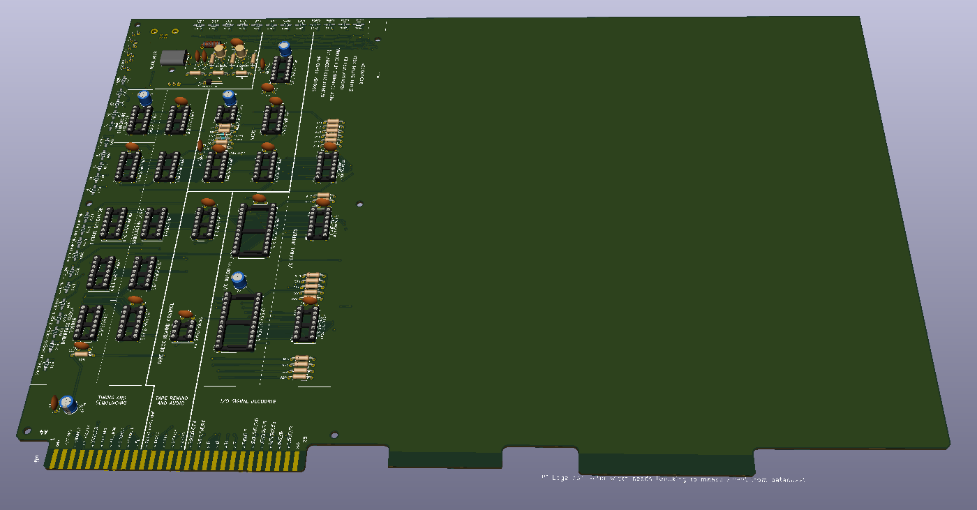
All components placed - to match the positions on the original board. Still some fettling to do on the edge connectors.
I'm now finally realising how ridiculously large this board is. In a way which, for unknown reasons, I'd been completely oblivious to previously.
#ttlprocessor #datapoint2200 #datapoint #d2200
Bread80 · @bread80
193 followers · 888 posts · Server mstdn.social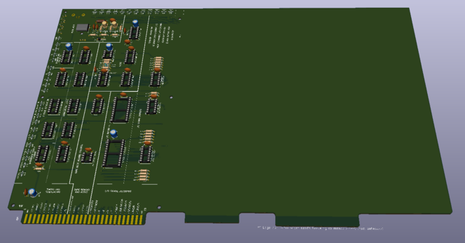
I've copied the Decoder PCB to get the edges of the Processor PCB. I'm using a print out of the decoder PCB and the long edge dimension of the decoder board to work out the scale of the print out.
I can then measure and scale up from the print out.
I'll keep the old decoder components and silk screen for the moment to reuse dimensions and design standards.
#ttlprocessor #datapoint2200 #datapoint #d2200
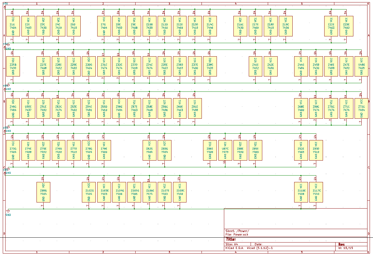
Bread80 · @bread80
193 followers · 888 posts · Server mstdn.social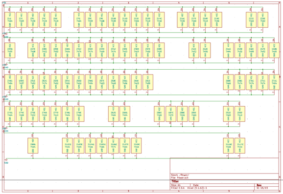
Now this is the dictionary definition of tedium. An entire page of power units for the logic gates.
Gaps are for chips with power connections on the main symbol. Not, BTW, the same as chips containing a single unit - there are several 8-input gates with one unit per chip but those still have a separate power unit.
#ttlprocessor #datapoint2200 #datapoint #d2200
Bread80 · @bread80
193 followers · 888 posts · Server mstdn.social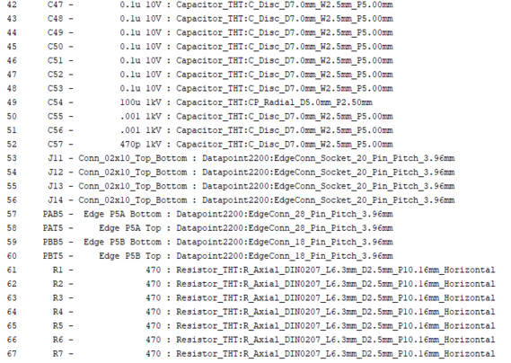
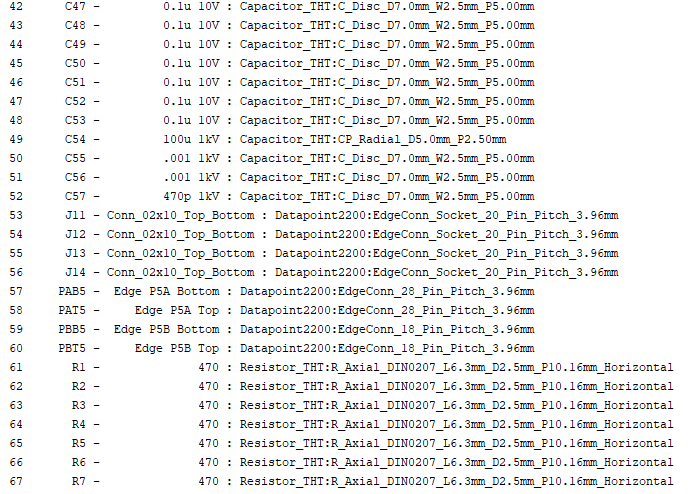
Adding footprints. No difficulty here. There's only 8 different footprints across the board: 3 for connectors; 2 for capacitors; 1 for resistors; and 2 for chips.
This was the early days of 74 series logic so only 14- and 16-pin packages in use.
#ttlprocessor #datapoint2200 #datapoint #d2200
Bread80 · @bread80
193 followers · 888 posts · Server mstdn.social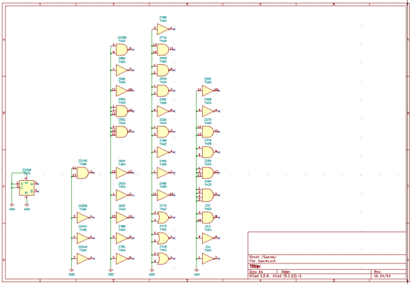
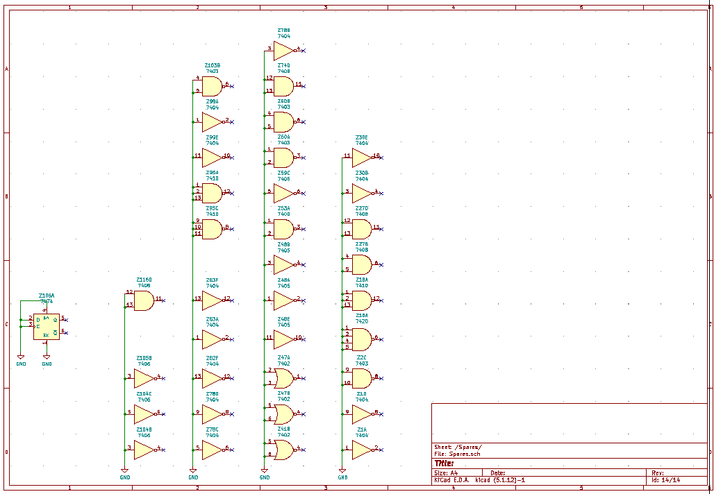
Adding a page of spare units, based off the table on the original schematics, but the design checker doesn't like it.
So, the original is hard to read, and I've not double checked what I've copied, but it clearly shows Z95 with some spare units. But Z95 is one of the RAM chips making up the stack. So this table is definitely error prone.
#ttlprocessor #datapoint2200 #datapoint #d2200
Bread80 · @bread80
193 followers · 860 posts · Server mstdn.social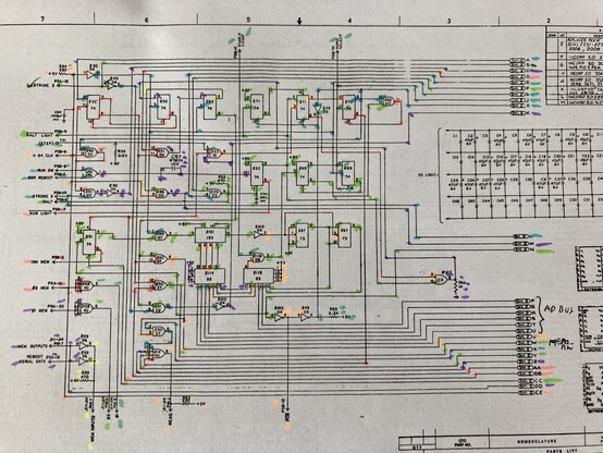
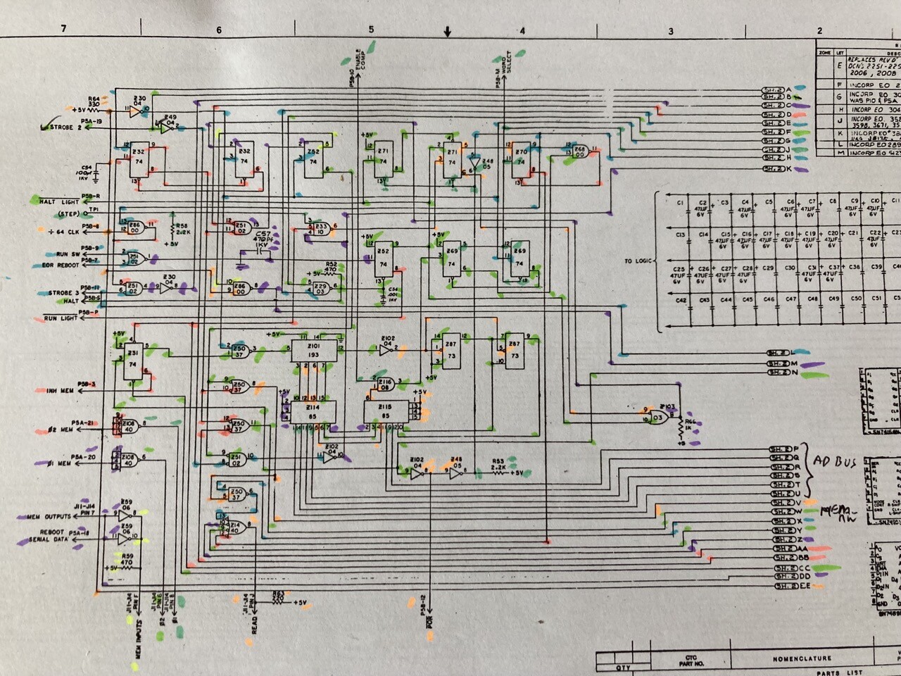
Current status: proof reading the schematics. I’m following every connection and using highlighter pens to mark where I’ve been. And doing the same to my schematics. The assortment of colours helps to stop me getting muddled.
Thus probably counts as tedious but my brain enjoys this kind of task.
#ttlprocessor #datapoint2200 #datapoint #d2200
Bread80 · @bread80
191 followers · 849 posts · Server mstdn.social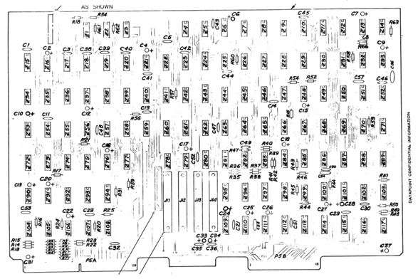
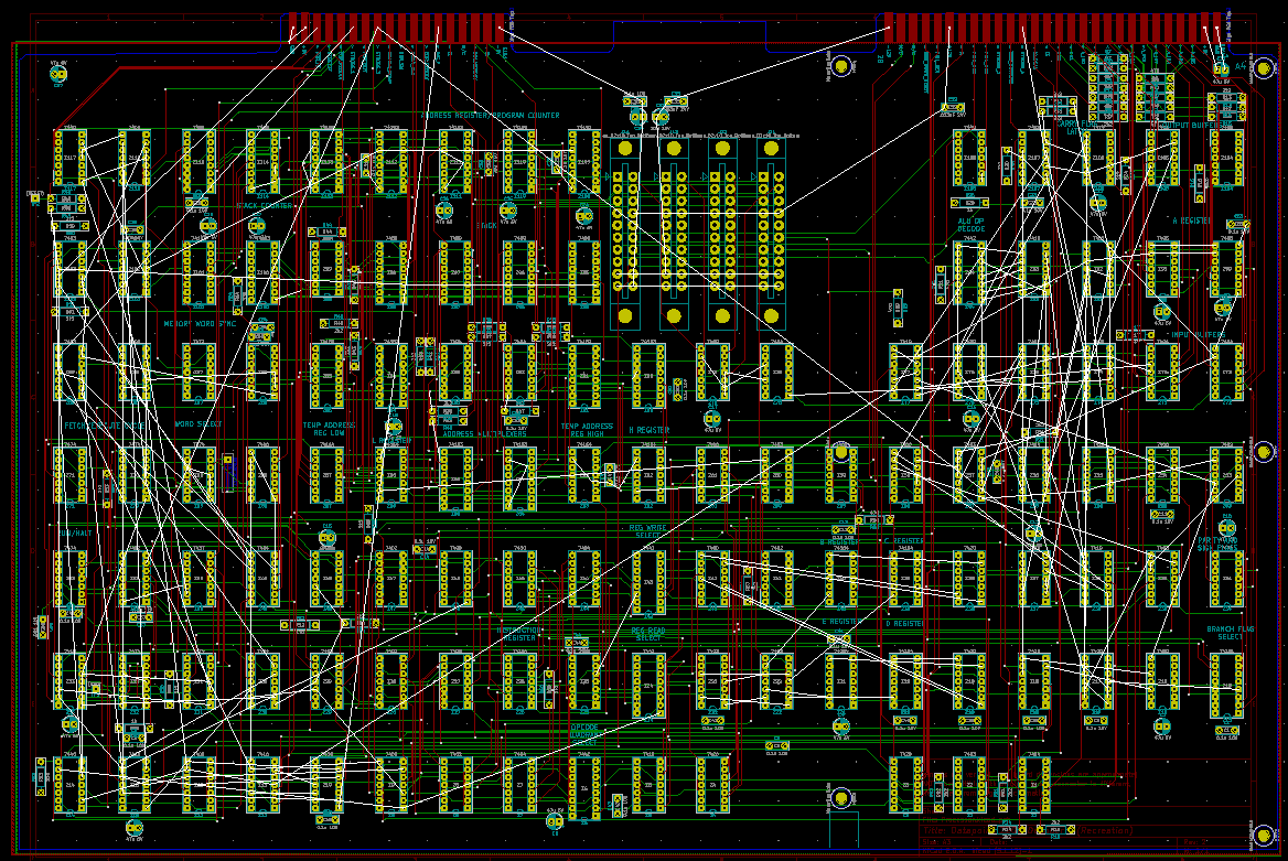
With the #Datapoint memory board sent to the fab it's time for the most exciting part of the project: the processor board.
This is A3 sized and houses 117 ICs. I'll be adding as many blinkenlights as I can fit.
I intend to toot as much as I can about the design process. I think it should be ... ahem ... interesting.
But it won't be quick. I'll be fitting it around other projects, and it'll be a ton of work anyway.
#ttlprocessor #datapoint2200 #d2200 #datapoint
Bread80 · @bread80
188 followers · 835 posts · Server mstdn.social
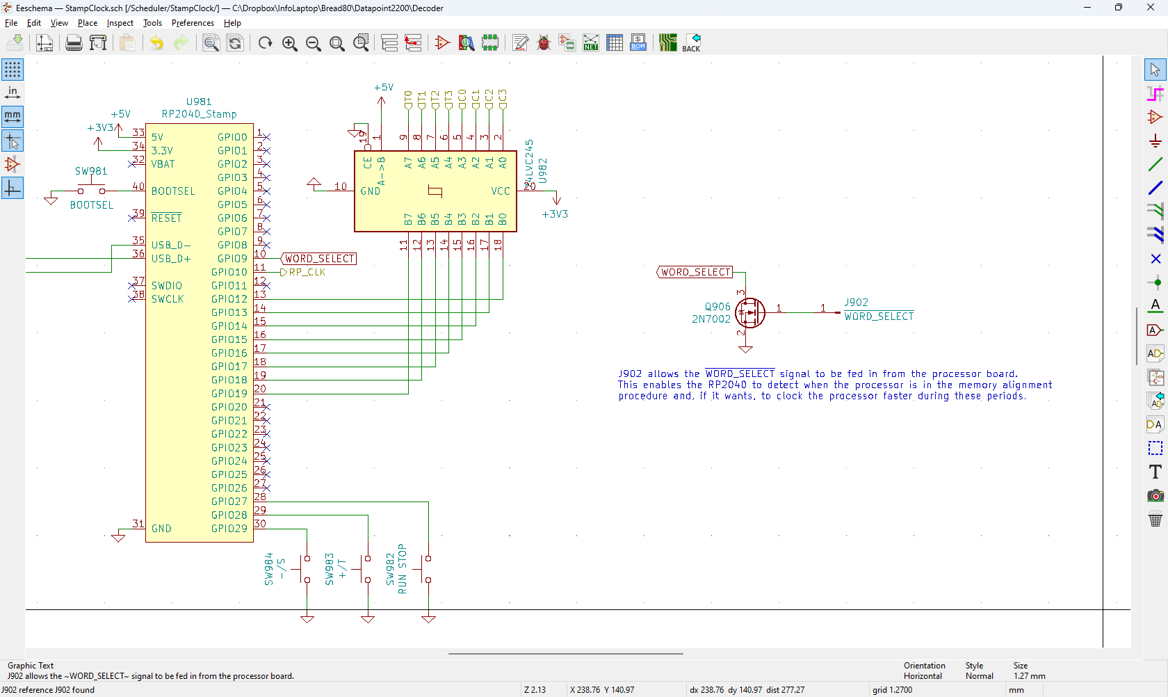
Returning to the #Datapoint 2200 project for the day. First up is adding a pin to the Decoder PCB so that the WORD_SELECT signal from the processor board can be fed into the controller that generates the clock.
To do a random memory read or write the processor has to rotate the shift memories to the address, then continue shifting them to get back to the execution address.
Each memory stores 64 bytes. Each instruction executes in the same time as rotating by two or three bytes. 1/n

The Hindu :press: · @the_hindu
169 followers · 679 posts · Server press.coopIn this week’s edition of the #DataPoint newsletter, @RebeccaRoseVar1 takes a look at the #gender gap in multiple healthcare domains including clinical trials, research funding as well as testing and diagnosis.
https://trib.al/AWLFVJD #press
Bread80 · @bread80
186 followers · 732 posts · Server mstdn.socialThe main purpose of this board is to divide the raw clock into ten steps. Eight of these clock memory, the other two are when the processor ‘does stuff’.
Each of these ten steps is then subdivided into four. This generates the two phase clock signals needed for the memory and other parts of the processor.
Since the machine has a one bit processor these signals also clock the internal shift registers, ALU, etc.
#datapoint 2200 #ttlprocessor
Bread80 · @bread80
183 followers · 685 posts · Server mstdn.social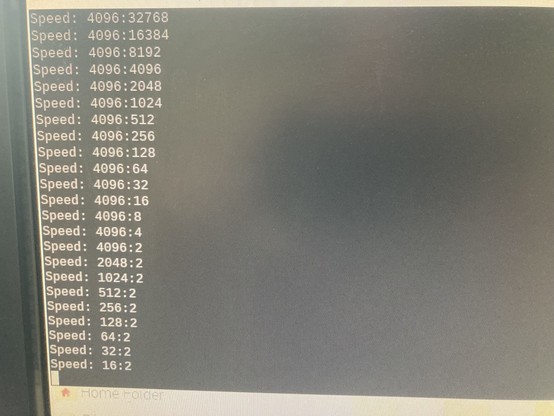
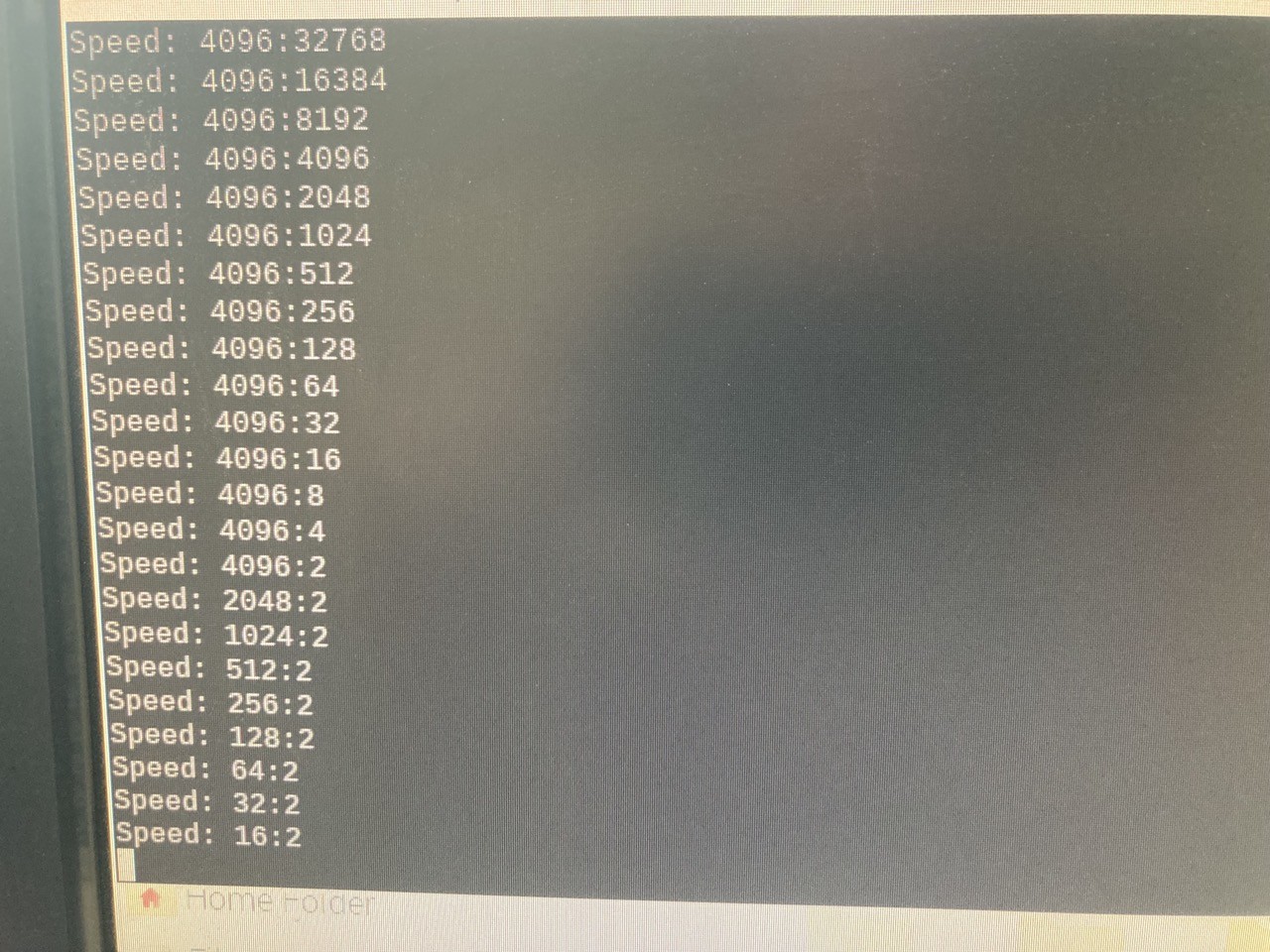
Doing some more work on the #datapoint 2200 decoder clock software for the RP2040.
Button scanning now runs off a 50Hz timer, so it’s not dependant on the speed of the main loop.
The actual clock generation now uses a PWM. I’m controlling the clock divider, top and level settings to set the PWM frequency. Screenshot shows the frequency increasing at each step to the maximum.
The Hindu :press: · @the_hindu
132 followers · 729 posts · Server press.coopWatch | February 2023 saw sea ice levels in #Antarctica fall to the lowest levels ever recorded. In this episode of #DataPoint, @sonikkalogan looks at how temperatures and sea ice cover has changed over the years, and what the impacts of this are.
https://trib.al/V5dUUQk #press
The Hindu :press: · @the_hindu
123 followers · 780 posts · Server press.coop#DataPoint | Earlier this month, the SC passed a ruling that allows the apex court to grant divorce in cases of irretrievable breakdown of marriage. @sonikkalogan speaks with Geeta Ramaseshan about whether this can help women leave unhealthy marriages.
The Hindu :press: · @the_hindu
121 followers · 806 posts · Server press.coop#DataPoint | Earlier this month, the SC passed a ruling that allows the apex court to grant divorce in cases of irretrievable breakdown of marriage. @sonikkalogan speaks with Geeta Ramaseshan about whether this can help women leave unhealthy marriages.